|
| [2025-05-28] |
Mastering Quad SPI Communication – Professional-Level Analysis and Measurement Solutions |
|
Quad SPI (Quad Serial Peripheral Interface) is a highly efficient serial communication protocol widely used for high-speed data transfer between microcontrollers (MCUs) and external flash memory. Compared to traditional SPI, Quad SPI significantly boosts data throughput via parallel transmission using six lines, meeting the speed and performance demands of modern embedded systems.This article utilizes the ZEROPLUS logic analyzer to perform practical Quad SPI communication tests, offering in-depth analysis of signal waveforms and timing characteristics to verify data transfer reliability and accuracy. Through real-world cases, we reveal the design consideration of sampling on the falling edge of the CLK by the master controller, and analyze how the Flash chip’s output delay (tCLQV) affects timing. We demonstrate how falling-edge sampling enhances data stability and communication accuracy. Furthermore, the integration of multi-channel signal monitoring, timing measurements, and packet analysis underscores the vital role of logic analyzers in firmware validation, communication debugging, and chip compatibility testing. These tools provide clear evidence and efficient solutions for embedded system development.
|
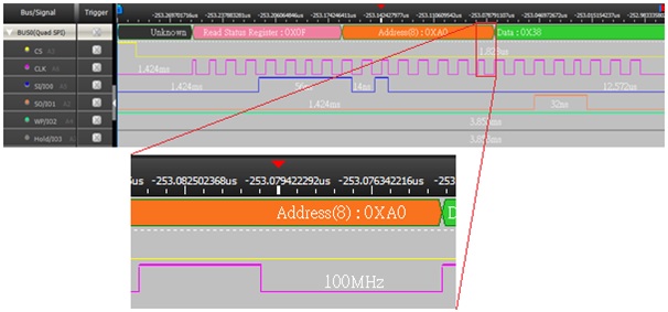 |
In this test, the ZEROPLUS logic analyzer is used to capture Quad SPI signal waveforms and precisely analyze timing characteristics to ensure that data bit transmission complies with external flash memory specifications. The built-in decoder can directly parse the signals into readable values and text, eliminating the tedious manual decoding process for engineers. The test results show:
- Command Decoding: Full parsing of Read/Write commands, such as 0x0F (read), 0x02 (lord program data), 0x06 (write enable).
- Field Explanation: Clearly displays address and data, e.g., Address: 0xA0, Data: 0x38.
- High-Frequency Analysis: Suitable for analyzing Quad SPI high-speed communication at 100 MHz.
- Data Verification: Confirms consistency between program data and subsequent Read Status Register results. |
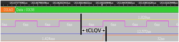 |
Through analysis, we observed that the master controller samples data on the falling edge of CLK, a design that accommodates the Flash chip's data output stabilization time after the rising edge. Falling-edge sampling not only improves data reliability but also increases timing tolerance. This feature can be verified using a logic analyzer and protocol decoder, which provides a clear foundation for debugging high-speed communication.
Further referencing the datasheet, the Flash chip’s data output delay (tCLQV) often exceeds half of the CLK cycle (tCH or tCL). If the master samples on the rising edge immediately, data might be misread due to instability. Therefore, system designs often delay the sampling point to the falling edge to allow more setup time and improve communication accuracy. This is especially critical in high-speed operations. Designers should refer to the Flash chip’s datasheet timing parameters and verify system reliability through actual measurement.
This case uses the Winbond W25N02KV, with tCLQV = 7 ns and an actual measured value of 6 ns, meeting the datasheet specifications. |
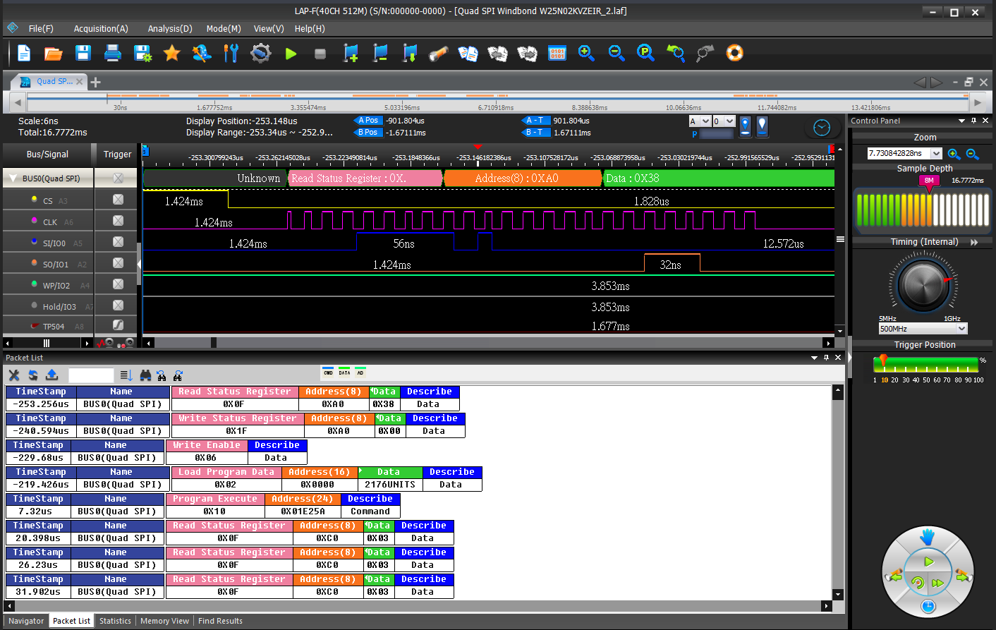 |
The ZEROPLUS logic analyzer is not just a testing tool—it is an indispensable source of visual evidence in embedded system development. |
|
|
|